- English
- French
- German
- Portuguese
- Spanish
- Russian
- Japanese
- Korean
- Arabic
- Greek
- German
- Turkish
- Italian
- Danish
- Romanian
- Indonesian
- Czech
- Afrikaans
- Swedish
- Polish
- Basque
- Catalan
- Esperanto
- Hindi
- Lao
- Albanian
- Amharic
- Armenian
- Azerbaijani
- Belarusian
- Bengali
- Bosnian
- Bulgarian
- Cebuano
- Chichewa
- Corsican
- Croatian
- Dutch
- Estonian
- Filipino
- Finnish
- Frisian
- Galician
- Georgian
- Gujarati
- Haitian
- Hausa
- Hawaiian
- Hebrew
- Hmong
- Hungarian
- Icelandic
- Igbo
- Javanese
- Kannada
- Kazakh
- Khmer
- Kurdish
- Kyrgyz
- Latin
- Latvian
- Lithuanian
- Luxembou..
- Macedonian
- Malagasy
- Malay
- Malayalam
- Maltese
- Maori
- Marathi
- Mongolian
- Burmese
- Nepali
- Norwegian
- Pashto
- Persian
- Punjabi
- Serbian
- Sesotho
- Sinhala
- Slovak
- Slovenian
- Somali
- Samoan
- Scots Gaelic
- Shona
- Sindhi
- Sundanese
- Swahili
- Tajik
- Tamil
- Telugu
- Thai
- Ukrainian
- Urdu
- Uzbek
- Vietnamese
- Welsh
- Xhosa
- Yiddish
- Yoruba
- Zulu
What Is A Hafnium Sputtering Target?
2025-02-17 16:02:59
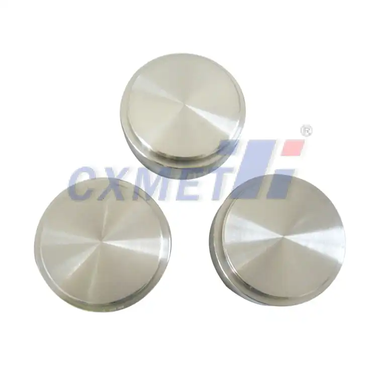
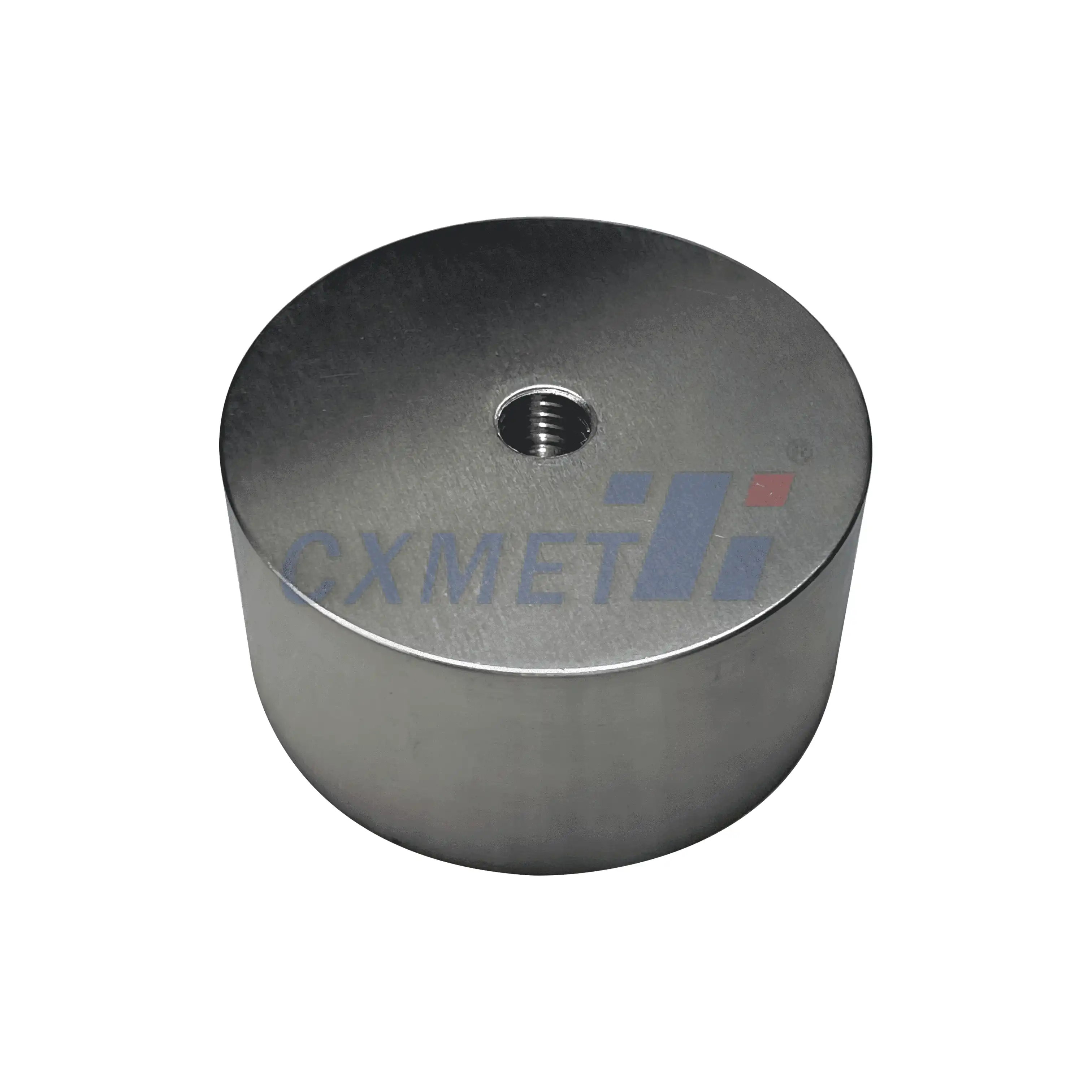
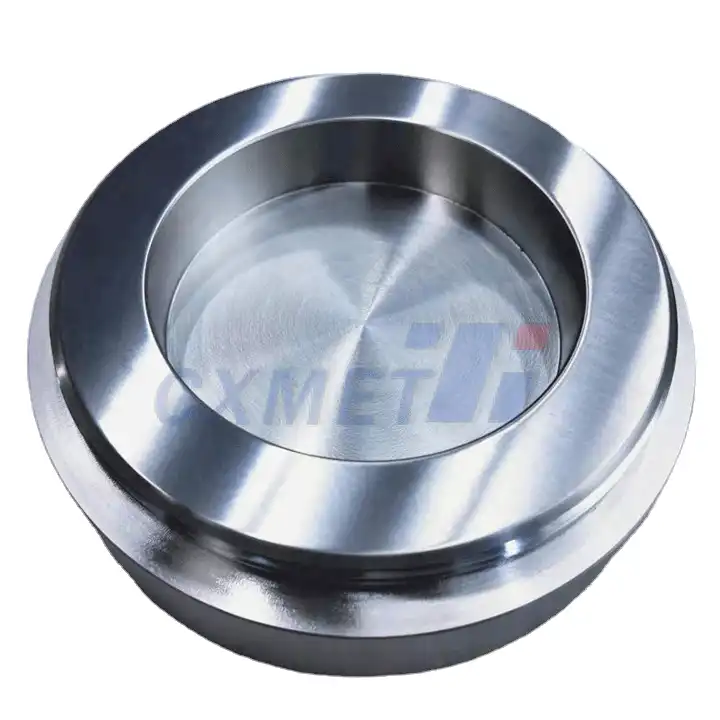
A hafnium sputtering target is a specialized material used in the physical vapor deposition (PVD) process known as sputtering. Hafnium, a transition metal with atomic number 72, is valued for its unique properties in various high-tech applications. In the form of a sputtering target, hafnium serves as the source material for depositing thin films of hafnium or hafnium-based compounds onto substrates. These targets are crucial in industries such as semiconductor manufacturing, optical coatings, and advanced materials research.


How is a hafnium sputtering target manufactured?
The manufacturing process of hafnium sputtering targets is a complex and precise procedure that requires specialized knowledge and equipment. It begins with the procurement of high-purity hafnium, typically in the form of hafnium sponge or crystal bar. The purity of the starting material is crucial, as any impurities can significantly affect the quality of the final thin film.
The first step in the manufacturing process is often the consolidation of the hafnium material. This can be achieved through various methods, including arc melting, electron beam melting, or powder metallurgy techniques. The choice of method depends on the desired final properties of the target and the specific requirements of the application.
Once the hafnium is consolidated, it undergoes a series of forming processes to achieve the desired shape and size for the sputtering target. This may involve techniques such as hot pressing, forging, or machining. The forming process is critical in ensuring the target has the correct dimensions and surface finish for optimal performance in the sputtering system.
After shaping, the target undergoes heat treatment processes to optimize its microstructure and properties. This step is crucial for achieving the desired density, grain structure, and mechanical properties that will affect the sputtering performance and target longevity.
The final stages of manufacturing involve precision machining and surface finishing. The target's surface must be extremely smooth and free of defects to ensure uniform sputtering and high-quality thin film deposition. Advanced techniques such as diamond turning or lapping may be employed to achieve the required surface finish.
Quality control is an integral part of the manufacturing process, with rigorous testing performed at various stages. This includes chemical analysis to verify purity, physical property measurements, and non-destructive testing methods to ensure the structural integrity of the target.
The manufacturing of hafnium sputtering targets often takes place in clean room environments to prevent contamination. The entire process is carefully controlled to maintain the high purity and specific properties required for advanced thin film applications.
What are the applications of hafnium sputtering targets?


Hafnium sputtering targets find applications in a wide range of high-tech industries due to the unique properties of hafnium and its compounds. One of the most significant applications is in the semiconductor industry, where hafnium-based materials have become essential in the production of advanced integrated circuits.
In semiconductor manufacturing, hafnium oxide (HfO2) has emerged as a critical material for high-k dielectrics in complementary metal-oxide-semiconductor (CMOS) transistors. As transistors have continued to shrink in size, traditional silicon dioxide gate dielectrics have reached their physical limits. Hafnium oxide, deposited using hafnium sputtering targets, offers higher dielectric constants while maintaining compatibility with silicon-based processes. This allows for thinner gate dielectrics, reducing leakage current and improving overall transistor performance.
Beyond semiconductors, hafnium sputtering targets are used in the production of optical coatings. Hafnium oxide and hafnium-based compounds exhibit excellent optical properties, including high refractive index and good transparency over a wide range of wavelengths. These characteristics make them ideal for creating anti-reflective coatings, dichroic filters, and other specialized optical components used in cameras, telescopes, and laser systems.
In the aerospace industry, hafnium-based coatings deposited using sputtering targets are employed to enhance the properties of turbine blades and other high-temperature components. Hafnium's high melting point and excellent resistance to corrosion make it valuable for protecting materials in extreme environments.
Hafnium sputtering targets also play a role in the development of advanced energy technologies. For instance, in nuclear reactors, hafnium is used as a neutron absorber in control rods. While not directly related to sputtering, the expertise gained in producing high-purity hafnium targets contributes to the overall advancement of hafnium metallurgy in various fields.
In the field of superconductivity research, hafnium-based compounds deposited using sputtering techniques are being explored for their potential in creating novel superconducting materials. This research could lead to breakthroughs in energy transmission and storage technologies.
How does the purity of a hafnium sputtering target affect its performance?
The purity of a hafnium sputtering target is a critical factor that significantly influences its performance and the quality of the resulting thin films. In the context of sputtering targets, purity refers to the absence of impurities and the concentration of the desired hafnium content. Typically, high-purity hafnium targets are specified at 99.9% (3N) purity or higher, with some advanced applications requiring 99.999% (5N) purity or even greater.
The impact of target purity on performance can be observed in several key areas. First and foremost, the purity directly affects the composition of the deposited film. Any impurities present in the target material will likely be incorporated into the thin film during the sputtering process. In applications such as semiconductor manufacturing, where the electrical and chemical properties of the film are crucial, even trace impurities can have significant detrimental effects on device performance.
For example, in the production of high-k dielectric layers using hafnium oxide, impurities can alter the dielectric constant, increase leakage current, or introduce trap states that degrade the performance of transistors. In optical applications, impurities can affect the refractive index or introduce absorption bands that compromise the desired optical properties of the coating.
The purity of the target also influences the sputtering process itself. Higher purity targets generally exhibit more uniform sputtering characteristics, leading to better control over deposition rates and film thickness uniformity. Impurities can cause localized variations in sputtering rates, potentially resulting in non-uniform film growth or the formation of defects in the deposited layer.
Moreover, the presence of certain impurities can affect the target's physical properties, such as its thermal conductivity or mechanical strength. This can impact the target's performance under high-power sputtering conditions and may reduce its overall lifespan. Higher purity targets often demonstrate better thermal management and resistance to cracking or other forms of degradation during use.
The choice of target purity is often a balance between performance requirements and cost considerations. While higher purity targets generally offer superior performance, they are also more expensive to produce. The specific purity level required depends on the application and the tolerance for impurities in the final product.
To ensure the desired purity levels are maintained, manufacturers of hafnium sputtering targets employ rigorous quality control measures. These may include advanced analytical techniques such as glow discharge mass spectrometry (GDMS), inductively coupled plasma mass spectrometry (ICP-MS), or secondary ion mass spectrometry (SIMS) to quantify trace impurities. Additionally, careful handling and storage procedures are implemented to prevent contamination during the manufacturing process and subsequent use.
At SHAANXI CXMET TECHNOLOGY CO., LTD, we take pride in our extensive product range, which caters to diverse customer needs. Our company is equipped with outstanding production and processing capabilities, ensuring the high quality and precision of our products. We are committed to innovation and continuously strive to develop new products, keeping us at the forefront of our industry. With leading technological development capabilities, we are able to adapt and evolve in a rapidly changing market. Furthermore, we offer customized solutions to meet the specific requirements of our clients. If you are interested in our products or wish to learn more about the intricate details of our offerings, please do not hesitate to contact us at sales@cxmet.com. Our team is always ready to assist you.

References
- Sarkar, J. (2014). Sputtering materials for VLSI and thin film devices. William Andrew.
- Depla, D., Mahieu, S., & Greene, J. E. (2010). Sputter deposition processes. In Handbook of deposition technologies for films and coatings (pp. 253-296). William Andrew Publishing.
- Wilk, G. D., Wallace, R. M., & Anthony, J. M. (2001). High-κ gate dielectrics: Current status and materials properties considerations. Journal of applied physics, 89(10), 5243-5275.
- Robertson, J. (2006). High dielectric constant gate oxides for metal oxide Si transistors. Reports on progress in physics, 69(2), 327.
- Choi, J. H., Mao, Y., & Chang, J. P. (2011). Development of hafnium based high-k materials—A review. Materials Science and Engineering: R: Reports, 72(6), 97-136.
- Nalwa, H. S. (Ed.). (2002). Handbook of thin film materials: deposition and processing of thin films (Vol. 1). Academic press.
- Mattox, D. M. (2010). Handbook of physical vapor deposition (PVD) processing. William Andrew.
- Swann, S. (1988). Magnetron sputtering. Physics in technology, 19(2), 67.
- Kelly, P. J., & Arnell, R. D. (2000). Magnetron sputtering: a review of recent developments and applications. Vacuum, 56(3), 159-172.
- Seshan, K. (Ed.). (2012). Handbook of thin film deposition. William Andrew.
YOU MAY LIKE