- English
- French
- German
- Portuguese
- Spanish
- Russian
- Japanese
- Korean
- Arabic
- Greek
- German
- Turkish
- Italian
- Danish
- Romanian
- Indonesian
- Czech
- Afrikaans
- Swedish
- Polish
- Basque
- Catalan
- Esperanto
- Hindi
- Lao
- Albanian
- Amharic
- Armenian
- Azerbaijani
- Belarusian
- Bengali
- Bosnian
- Bulgarian
- Cebuano
- Chichewa
- Corsican
- Croatian
- Dutch
- Estonian
- Filipino
- Finnish
- Frisian
- Galician
- Georgian
- Gujarati
- Haitian
- Hausa
- Hawaiian
- Hebrew
- Hmong
- Hungarian
- Icelandic
- Igbo
- Javanese
- Kannada
- Kazakh
- Khmer
- Kurdish
- Kyrgyz
- Latin
- Latvian
- Lithuanian
- Luxembou..
- Macedonian
- Malagasy
- Malay
- Malayalam
- Maltese
- Maori
- Marathi
- Mongolian
- Burmese
- Nepali
- Norwegian
- Pashto
- Persian
- Punjabi
- Serbian
- Sesotho
- Sinhala
- Slovak
- Slovenian
- Somali
- Samoan
- Scots Gaelic
- Shona
- Sindhi
- Sundanese
- Swahili
- Tajik
- Tamil
- Telugu
- Thai
- Ukrainian
- Urdu
- Uzbek
- Vietnamese
- Welsh
- Xhosa
- Yiddish
- Yoruba
- Zulu
Why Is Hafnium Used In Sputtering Targets?
2025-02-19 17:02:37
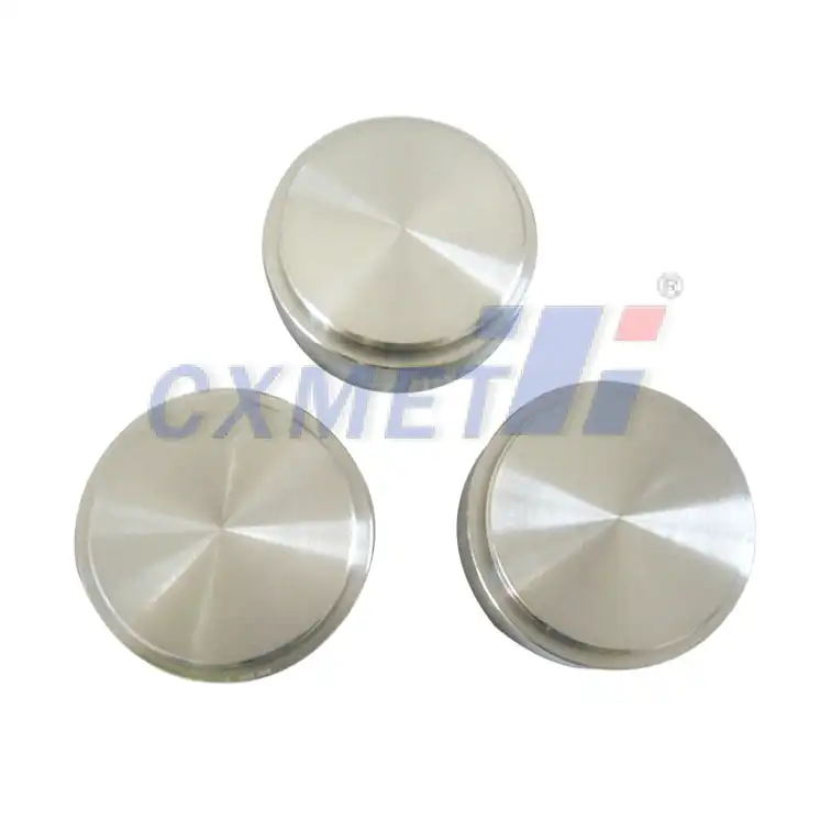
Hafnium, a silvery-white transition metal, has gained significant importance in the field of thin film deposition, particularly in sputtering applications. Its unique properties make it an ideal material for hafnium sputtering targets, which are essential components in various industries, including semiconductor manufacturing, optical coatings, and advanced materials research. This blog post will explore the reasons behind hafnium's popularity in sputtering targets and delve into its applications and advantages.


What are the unique properties of hafnium that make it suitable for sputtering targets?
Hafnium possesses several distinctive properties that make it an excellent choice for sputtering targets. These characteristics contribute to its effectiveness in thin film deposition processes and enable the production of high-quality coatings. Let's examine some of the key properties that set hafnium apart:
- High melting point: Hafnium has a melting point of approximately 2,233°C (4,051°F), which is significantly higher than many other materials used in sputtering targets. This high melting point allows hafnium to withstand the intense heat generated during the sputtering process without degrading or deforming.
- Excellent thermal stability: In addition to its high melting point, hafnium exhibits remarkable thermal stability. This property ensures that the target maintains its structural integrity and composition even under prolonged exposure to high temperatures during sputtering.
- Low vapor pressure: Hafnium has a relatively low vapor pressure, which is advantageous in sputtering applications. This characteristic helps minimize contamination of the deposited film by reducing the likelihood of unwanted evaporation or sublimation of the target material.
- High density: With a density of approximately 13.31 g/cm³, hafnium is a dense material. This high density contributes to efficient sputtering rates and allows for the production of uniform and dense thin films.
- Chemical stability: Hafnium is known for its excellent chemical stability, particularly its resistance to corrosion and oxidation. This property ensures that the sputtering target remains stable during storage and use, maintaining its purity and performance over time.
- Compatibility with other materials: Hafnium can be easily alloyed or combined with other elements, making it versatile for creating composite or multi-component sputtering targets. This compatibility allows for the tailoring of target compositions to meet specific thin film requirements.
These unique properties collectively contribute to hafnium's suitability as a sputtering target material. Its ability to withstand high temperatures, maintain stability, and produce high-quality thin films makes it an attractive choice for various applications in the semiconductor and electronics industries.
How does hafnium compare to other materials used in sputtering targets?
When comparing hafnium to other materials commonly used in sputtering targets, several factors come into play. To understand hafnium's position in the hierarchy of sputtering target materials, it's essential to consider its performance relative to alternatives such as titanium, tantalum, and zirconium. Let's explore how hafnium compares in various aspects:
- Melting point: Hafnium's high melting point (2,233°C) is comparable to that of tantalum (3,017°C) and higher than titanium (1,668°C) and zirconium (1,855°C). This high melting point allows hafnium targets to maintain their integrity during high-power sputtering processes.
- Sputtering yield: The sputtering yield of hafnium is generally lower than that of lighter elements like titanium but higher than heavier elements like tantalum. This moderate yield allows for controlled deposition rates and good film uniformity.
- Density: Hafnium's density (13.31 g/cm³) is higher than titanium (4.51 g/cm³) and zirconium (6.52 g/cm³) but lower than tantalum (16.69 g/cm³). This relatively high density contributes to efficient momentum transfer during sputtering and helps achieve good film adhesion.
- Chemical reactivity: Compared to titanium and zirconium, hafnium is less reactive, which can be advantageous in certain applications where minimal interaction with residual gases in the sputtering chamber is desired. However, it is more reactive than noble metals like platinum or gold.
- Cost: Hafnium is generally more expensive than titanium and zirconium but less costly than some precious metals used in sputtering targets. Its price point often positions it as a premium material for specialized applications.
- Electrical resistivity: Hafnium has a higher electrical resistivity compared to more conductive metals like copper or aluminum. This property can be beneficial in certain electronic applications where higher resistivity is required.
- Oxidation resistance: Hafnium forms a stable oxide layer, providing good oxidation resistance. This characteristic is similar to zirconium but superior to titanium in high-temperature applications.
When choosing a sputtering target material, the specific requirements of the application must be considered. Hafnium's unique combination of properties makes it particularly suitable for applications in the semiconductor industry, where high-quality, high-k dielectric films are required. Its ability to form stable oxides with high dielectric constants gives it an edge over materials like titanium or aluminum in certain electronic device fabrications.
Moreover, hafnium's compatibility with other materials allows for the creation of alloy targets, such as hafnium-silicon or hafnium-tantalum, which can be tailored to meet specific thin film composition requirements. This versatility in alloying further expands its range of applications compared to single-element targets.
In summary, while each material has its strengths, hafnium occupies a unique position in the spectrum of sputtering target materials. Its balance of thermal stability, moderate sputtering yield, and chemical properties makes it an excellent choice for applications requiring high-quality, stable thin films, particularly in advanced semiconductor and electronic device manufacturing.
What are the main applications of hafnium sputtering targets in the semiconductor industry?
Hafnium sputtering targets have found numerous applications in the semiconductor industry, primarily due to their unique properties and the high-quality thin films they can produce. The use of hafnium in this field has grown significantly in recent years, particularly as the industry moves towards smaller and more efficient electronic devices. Let's explore some of the main applications of hafnium sputtering targets in semiconductor manufacturing:
- High-k dielectric layers: One of the most significant applications of hafnium in the semiconductor industry is in the production of high-k dielectric layers. As transistors have continued to shrink, traditional silicon dioxide gate dielectrics have reached their physical limits. Hafnium-based dielectrics, such as hafnium oxide (HfO2), have emerged as an excellent alternative due to their higher dielectric constant. This property allows for thicker physical layers while maintaining the same electrical characteristics, reducing leakage current and improving overall device performance.
- Metal gate electrodes: In addition to high-k dielectrics, hafnium is also used in metal gate electrodes. When combined with other metals, hafnium can help create gate electrodes with the appropriate work function for both NMOS and PMOS transistors. This application is crucial in the development of advanced CMOS (Complementary Metal-Oxide-Semiconductor) technology.
- Diffusion barriers: Hafnium and its compounds can serve as effective diffusion barriers in semiconductor devices. These barriers prevent the migration of atoms between different layers of the device, which is essential for maintaining the integrity and performance of integrated circuits.
- Optical coatings: While not strictly a semiconductor application, hafnium-based thin films are used in the production of optical coatings for semiconductor manufacturing equipment. These coatings can enhance the performance and durability of optical components used in lithography systems and other semiconductor processing tools.
- Resistive memory devices: Hafnium oxide has shown promise in the development of resistive random-access memory (RRAM) devices. These next-generation memory technologies could potentially offer higher storage densities and lower power consumption compared to current memory technologies.
- Ferroelectric devices: Recent research has revealed that certain phases of hafnium oxide exhibit ferroelectric properties. This discovery has opened up new possibilities for hafnium in the development of ferroelectric field-effect transistors (FeFETs) and other novel device structures.
- Doping and alloying: Hafnium can be used as a dopant or alloying element in various semiconductor materials to modify their electrical, optical, or structural properties. This versatility allows for the fine-tuning of material characteristics to meet specific device requirements.
The use of hafnium sputtering targets in these applications offers several advantages:
- Improved device performance: Hafnium-based high-k dielectrics and metal gates enable the continued scaling of transistors, leading to faster and more energy-efficient devices.
- Enhanced reliability: The stability and durability of hafnium-based films contribute to improved device reliability and longer operational lifetimes.
- Compatibility with existing processes: Hafnium can often be integrated into existing semiconductor manufacturing processes with minimal modifications, facilitating its adoption in production environments.
- Scalability: As the semiconductor industry continues to push towards smaller node sizes, hafnium-based materials have demonstrated good scalability, making them suitable for future technology nodes.
As the semiconductor industry continues to evolve, the role of hafnium sputtering targets is likely to expand further. Ongoing research into new hafnium-based materials and device structures promises to unlock even more applications for this versatile element in the realm of advanced electronics and semiconductor manufacturing.
At SHAANXI CXMET TECHNOLOGY CO., LTD, we take pride in our extensive product range, which caters to diverse customer needs. Our company is equipped with outstanding production and processing capabilities, ensuring the high quality and precision of our products. We are committed to innovation and continuously strive to develop new products, keeping us at the forefront of our industry. With leading technological development capabilities, we are able to adapt and evolve in a rapidly changing market. Furthermore, we offer customized solutions to meet the specific requirements of our clients. If you are interested in our products or wish to learn more about the intricate details of our offerings, please do not hesitate to contact us at sales@cxmet.com. Our team is always ready to assist you.


References
- Wang, X., et al. (2018). Hafnium-based high-k gate dielectrics. In Handbook of Thin Film Deposition (pp. 283-326). William Andrew Publishing.
- Kaloyeros, A. E., & Eisenbraun, E. (2000). Ultrathin diffusion barriers/liners for gigascale copper metallization. Annual Review of Materials Science, 30(1), 363-385.
- Miikkulainen, V., et al. (2013). Crystallinity of inorganic films grown by atomic layer deposition: Overview and general trends. Journal of Applied Physics, 113(2), 021301.
- Robertson, J. (2006). High dielectric constant gate oxides for metal oxide Si transistors. Reports on Progress in Physics, 69(2), 327.
- Böscke, T. S., et al. (2011). Ferroelectricity in hafnium oxide thin films. Applied Physics Letters, 99(10), 102903.
- Tan, Y. N., et al. (2007). Hafnium-doped tantalum oxide high-k dielectric films for CMOS applications. Journal of Applied Physics, 102(10), 104101.
- Choi, J. H., et al. (2018). Hafnium oxide-based resistive switching materials and devices for neuromorphic computing. Journal of Materials Chemistry C, 6(23), 6146-6161.
- Kittl, J. A., et al. (2009). High-k dielectrics for future generation memory devices. Microelectronic Engineering, 86(7-9), 1789-1795.
- Wong, H. S. P., & Salahuddin, S. (2015). Memory leads the way to better computing. Nature Nanotechnology, 10(3), 191-194.
- Jiang, B., et al. (2018). Hafnium-based thin films in high-k gate dielectric applications: A review. Applied Physics Reviews, 5(2), 021303.
YOU MAY LIKE